The AI race is usually described through the companies developing models and selling computing systems.
Nvidia, OpenAI, Anthropic, Google, Microsoft, and other technology companies occupy the visible layer of the industry. Behind them sits a more basic dependency: the advanced semiconductor.
An AI chip is not produced by one company or within one national economy. It is the final output of a distributed industrial system involving chip architecture, processor design, specialized software, lithography, precision optics, deposition, etching, inspection, fabrication, memory, packaging, electricity, cooling, and data-center infrastructure.
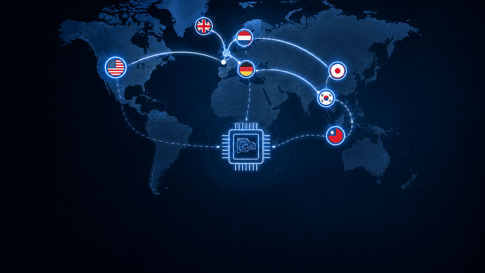
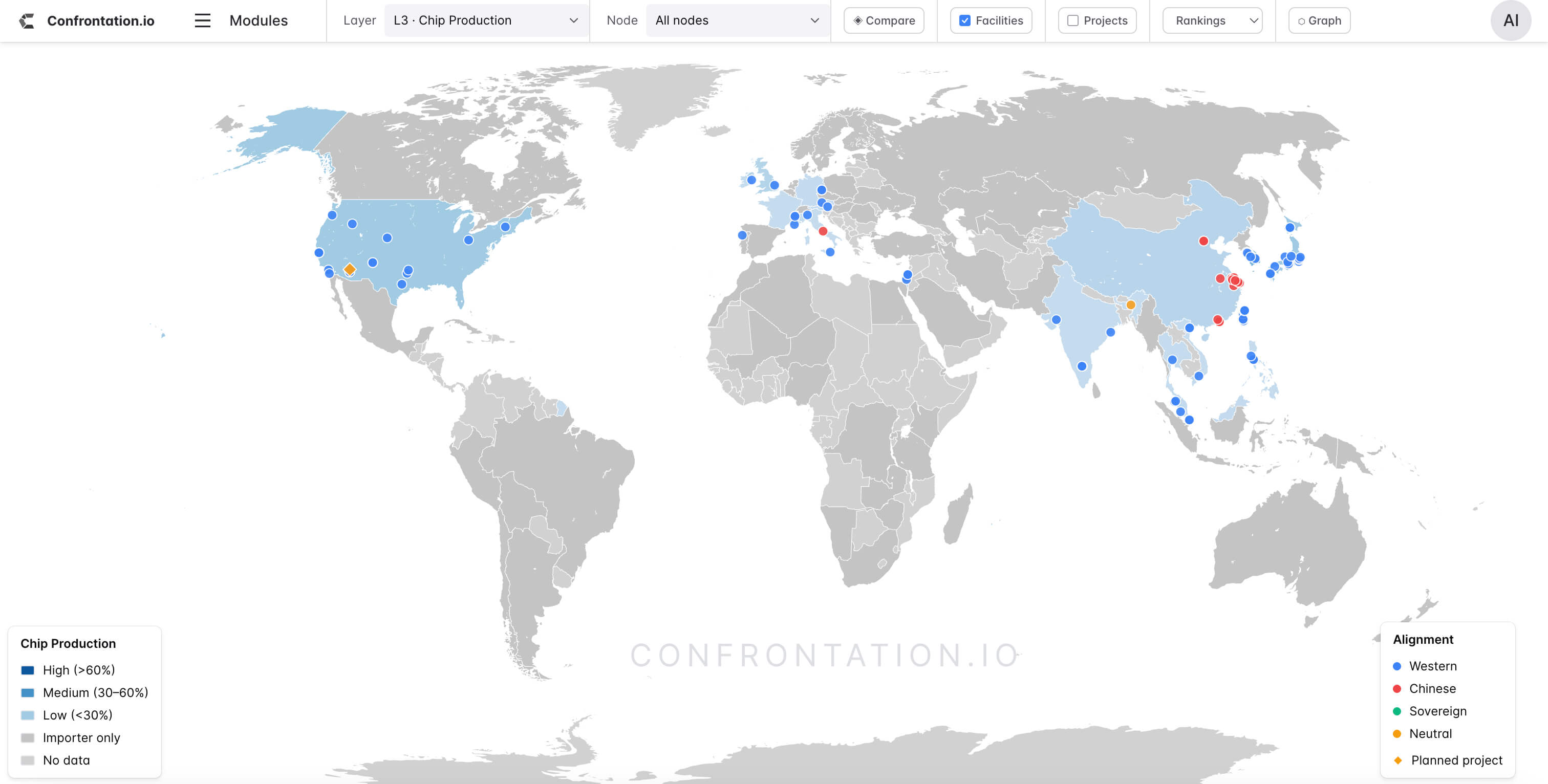
Different parts of this system are concentrated in different countries. The United States leads much of advanced chip design and semiconductor software. The United Kingdom remains influential in processor architecture. The Netherlands and Germany occupy central positions in advanced lithography and optics. The United States and Japan supply large parts of the wider manufacturing-equipment ecosystem. Taiwan dominates the integration of these technologies through advanced fabrication and packaging. South Korea is central to high-bandwidth memory.
The result resembles an alliance, although not one created through a formal treaty.
It is an industrial alliance composed of companies, governments, suppliers, research institutions, fabrication plants, infrastructure networks, export regulations, intellectual property, and decades of accumulated manufacturing experience.
Its strength comes from specialization. Its vulnerability comes from concentration.
At almost every stage of the AI-chip journey, a small number of companies occupy positions that are difficult to replace. Their advantages were built through engineering knowledge, supplier relationships, patents, capital investment, process data, and experience operating at industrial scale.
This is where business becomes geopolitics.
When one company or country controls a critical layer of the semiconductor chain, it gains influence over everyone who depends on that layer. The AI race therefore begins long before a model is trained or a data center is built. It begins inside the industrial system that turns a digital chip design into physical computing capacity.
The Semiconductor Production Chain
The production of an advanced AI processor begins with architecture and design.
Engineers must define how the processor will operate, organize billions of transistors, design memory controllers, construct communication pathways, and determine how data will move across the finished chip.
The design must then be tested through specialized software. Engineers simulate how the processor will behave, identify logical and physical problems, verify power consumption, estimate thermal performance, and determine whether the design can be manufactured using available semiconductor processes.
Once the digital design is complete, it must be transferred onto silicon.
Lithography systems project extremely small circuit patterns onto a wafer. Deposition tools add thin material layers. Etching systems remove selected material. Cleaning equipment prevents contamination. Inspection and metrology systems measure defects and verify whether each stage of the process remains within narrow tolerances.
A fabrication plant must coordinate all of these systems across hundreds or thousands of individual process steps.
The completed wafer is then divided into individual processor dies. These dies must be connected to high-bandwidth memory and placed into an advanced package capable of moving enormous volumes of data between components.
Only after this process does the finished accelerator enter a server. It must then be connected to networking equipment, installed in a data-center rack, supplied with electricity, and cooled continuously before it can train or operate an AI model.
Each stage represents a separate industrial layer. Each layer has its own technical barriers, leading companies, geographic concentrations, and political dependencies.
Architecture and Chip Design
The first stage exists entirely in digital form.
Chip architects determine the basic structure of the processor. They define the instruction systems, computing units, memory interfaces, data pathways, and specialized functions required for a particular workload.
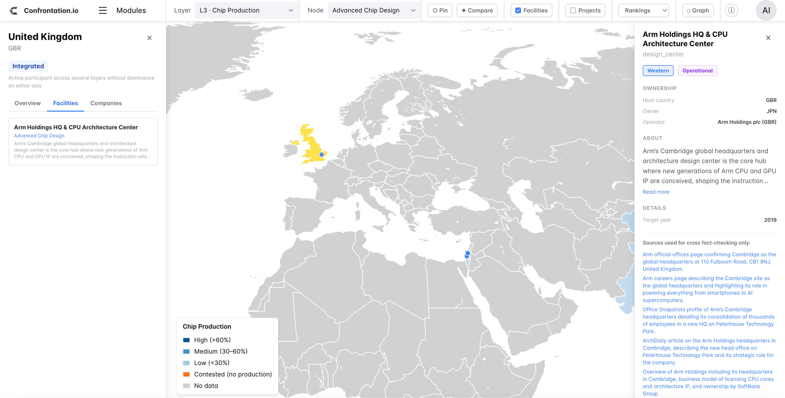
The United Kingdom remains important at this level through Arm, whose processor architectures and intellectual property are widely used across mobile devices, embedded systems, cloud infrastructure, and increasingly specialized computing platforms.
Arm does not manufacture most of the processors based on its architecture. Instead, it licenses designs and technical building blocks to other companies. This allows chip developers to construct products without creating every component of the processor architecture independently.
The United States dominates much of the advanced chip-design layer.
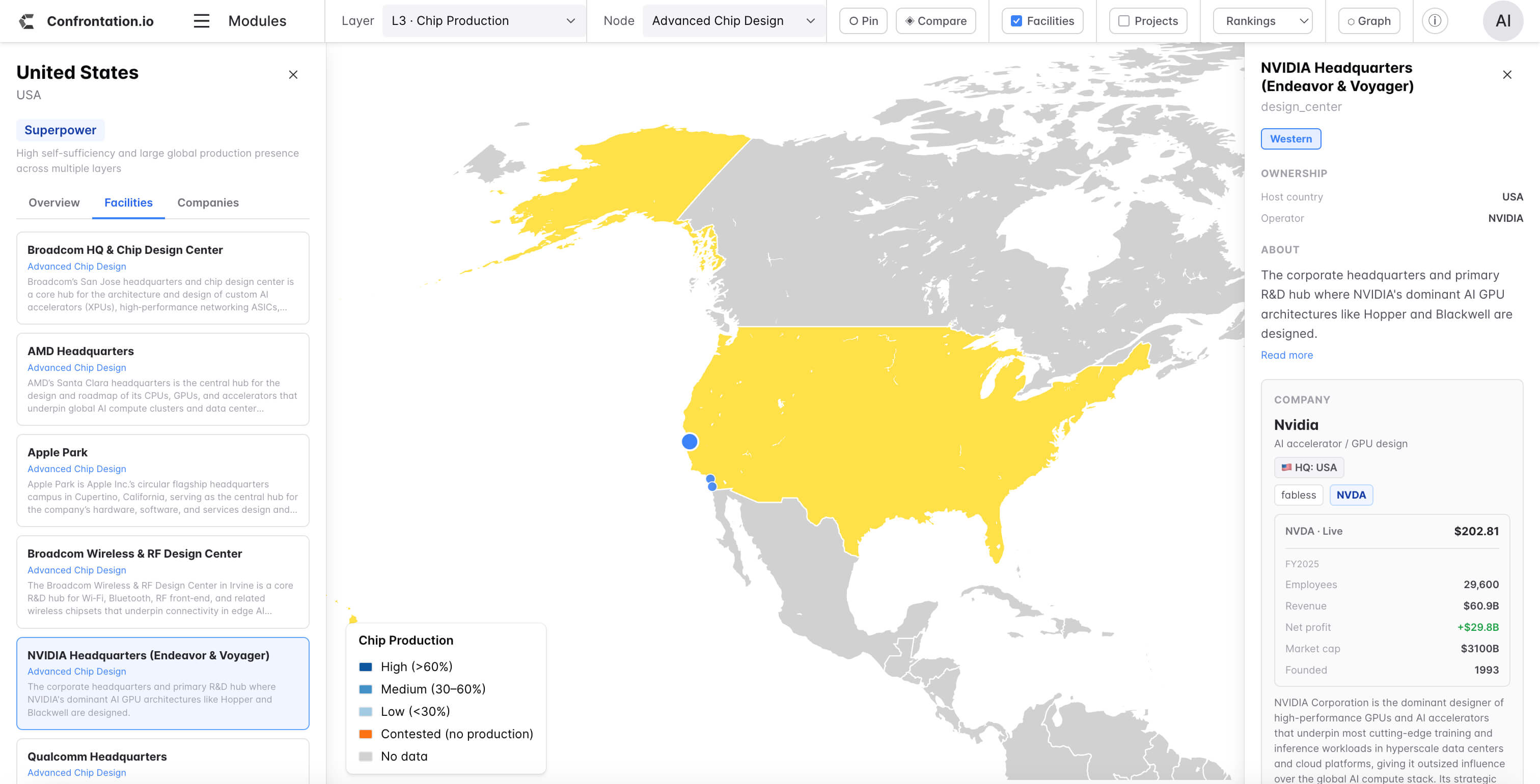
Nvidia designs the accelerators that currently support a large share of frontier AI training and inference. AMD produces competing processors and computing platforms. Broadcom develops networking, connectivity, and custom semiconductor technologies used across data centers and communications infrastructure.
Other companies participate through different parts of the ecosystem. Qualcomm has extensive expertise in power-efficient processors and communications systems. Marvell develops networking and data-infrastructure chips. Apple designs processors for its consumer-computing ecosystem. Amazon, Google, Microsoft, and other cloud providers increasingly develop custom silicon for internal workloads.
These companies are frequently described as chipmakers, although many do not manufacture chips themselves.
They operate through a fabless model. The company designs the processor but relies on an external foundry to manufacture it.
This separation between design and production allows firms to specialize. A chip company can focus on architecture, software integration, and product development without owning fabrication plants that cost tens of billions of dollars to build and continuously upgrade.
The model also creates dependency. A successful design remains only a digital blueprint until another part of the industrial system can manufacture it.
The Software Behind the Design
Advanced chips cannot be designed manually.
Modern processors contain billions of transistors arranged across multiple layers. The physical layout must account for electrical behavior, timing, power consumption, heat, manufacturing rules, and the possibility of defects.
This creates a separate dependency on Electronic Design Automation software.
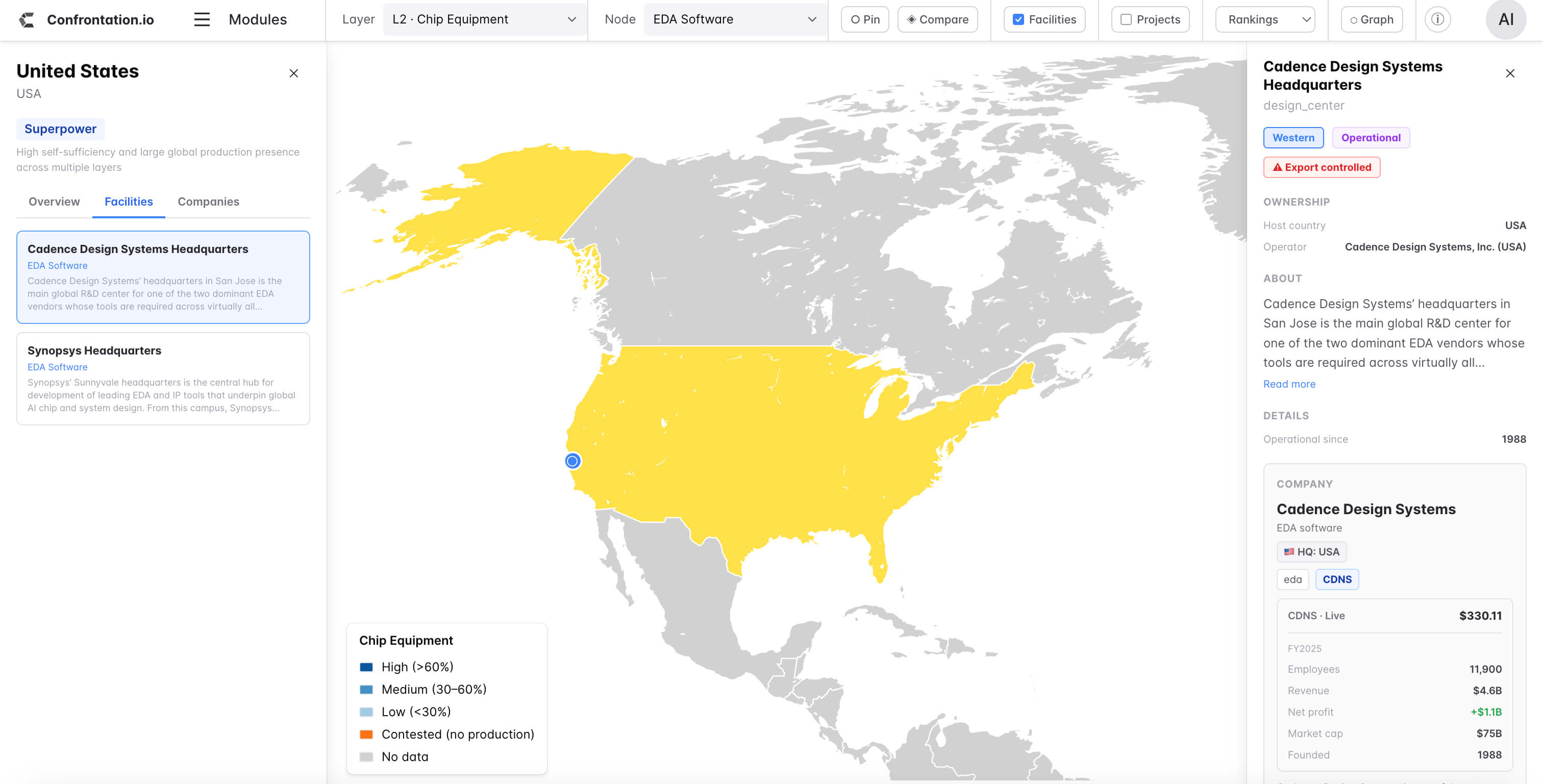
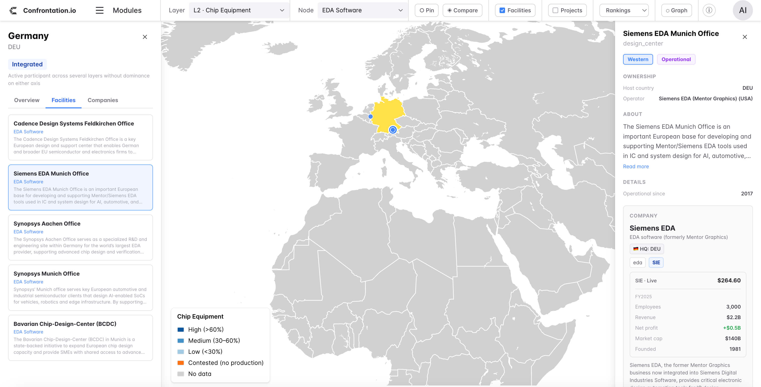
Synopsys and Cadence, both based in the United States, are leading suppliers of the tools used to design, simulate, verify, and prepare advanced processors for manufacturing. Siemens EDA, part of the German industrial group Siemens, is another major participant.
EDA software helps engineers translate a proposed chip architecture into a physical design that can be manufactured. It tests whether signals will arrive at the correct time, whether circuits will operate as expected, whether power requirements remain manageable, and whether the design follows the technical rules of the intended fabrication process.
These systems also connect chip designers with foundries.
A fabrication plant does not simply receive a generic digital file. The design must be adapted to the foundry’s specific production process, equipment configuration, materials, transistor structures, and manufacturing tolerances.
This creates close technical relationships between design-software companies, chip developers, and semiconductor foundries.
The EDA layer illustrates how industrial and government power overlap. Private companies create and maintain the software, while governments regulate intellectual property, exports, investment, and access to advanced tools.
Restrictions on design software can influence which companies are able to develop leading-edge processors, even before manufacturing equipment enters the picture.
By the end of this stage, the AI chip exists as a verified digital blueprint.
Turning that blueprint into a physical semiconductor requires a different industrial ecosystem built around some of the most sophisticated manufacturing tools ever created.
Lithography and the Equipment Ecosystem
Lithography is the most visible part of advanced semiconductor manufacturing.
A lithography system transfers circuit patterns onto silicon wafers by exposing light-sensitive materials through a highly controlled optical process. The smaller and more precise the projected pattern, the more advanced the resulting semiconductor can become.
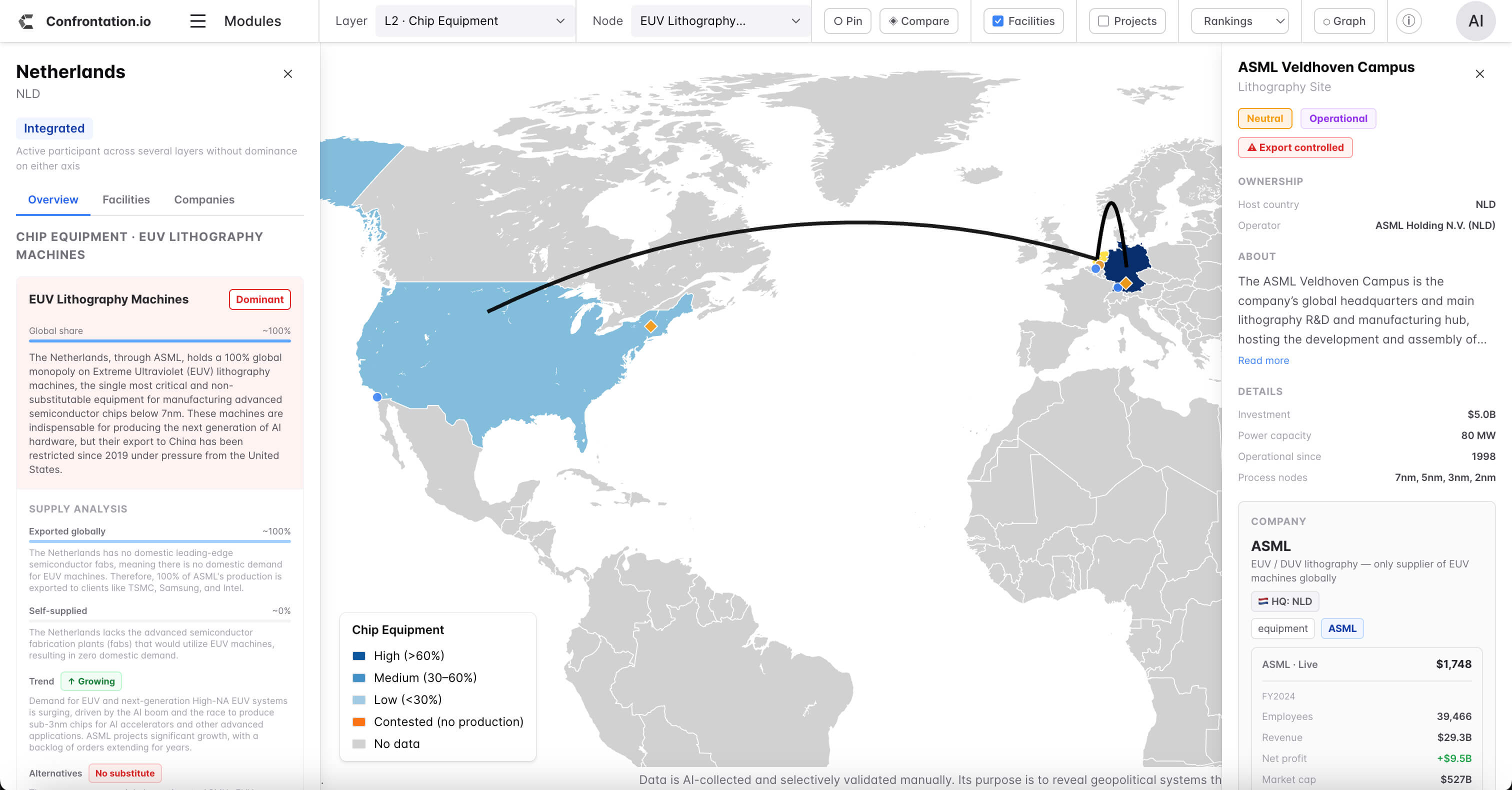
ASML, based in the Netherlands, is the central company in this layer.
Its extreme ultraviolet lithography systems are required for efficient production at the most advanced process nodes. These machines use light with an extremely short wavelength to print smaller features onto silicon.
The machines are often described as ASML products, although ASML operates more accurately as a system integrator at the center of a large international supplier network.
One of the most important suppliers is Carl Zeiss SMT in Germany. Zeiss produces the precision optical systems used to direct and control light inside advanced lithography machines.
The mirrors used in EUV lithography must operate at extraordinary levels of precision. Small imperfections can distort the projected pattern and reduce manufacturing yields.
The light source creates another technical challenge.
Cymer, a United States company acquired by ASML, developed important light-source technologies used in advanced lithography. Trumpf in Germany contributes high-powered laser systems required to generate the plasma process associated with EUV light production.
The result is not a purely Dutch machine.
It is a multinational industrial system combining Dutch integration, German optics and lasers, American light-source technology, specialized materials, software, vacuum systems, precision stages, and thousands of components supplied by companies across allied economies.
Governments influence this layer through export licensing.
The Dutch government controls the export of selected ASML systems. The United States shapes the wider control regime around advanced chips, manufacturing tools, software, and technical support. Germany and Japan also regulate equipment and components considered strategically important.
Lithography therefore provides one of the clearest examples of industrial concentration becoming geopolitical leverage.
Access to advanced machines affects whether a country can expand leading-edge semiconductor manufacturing through established global supply chains.
Lithography, however, is only one part of the fabrication process.
Building and Removing Material
A semiconductor factory constructs a chip through repeated cycles of adding, modifying, and removing material.
Deposition systems place extremely thin layers onto the wafer. These layers eventually form transistor structures, electrical connections, insulating barriers, and other components of the processor.
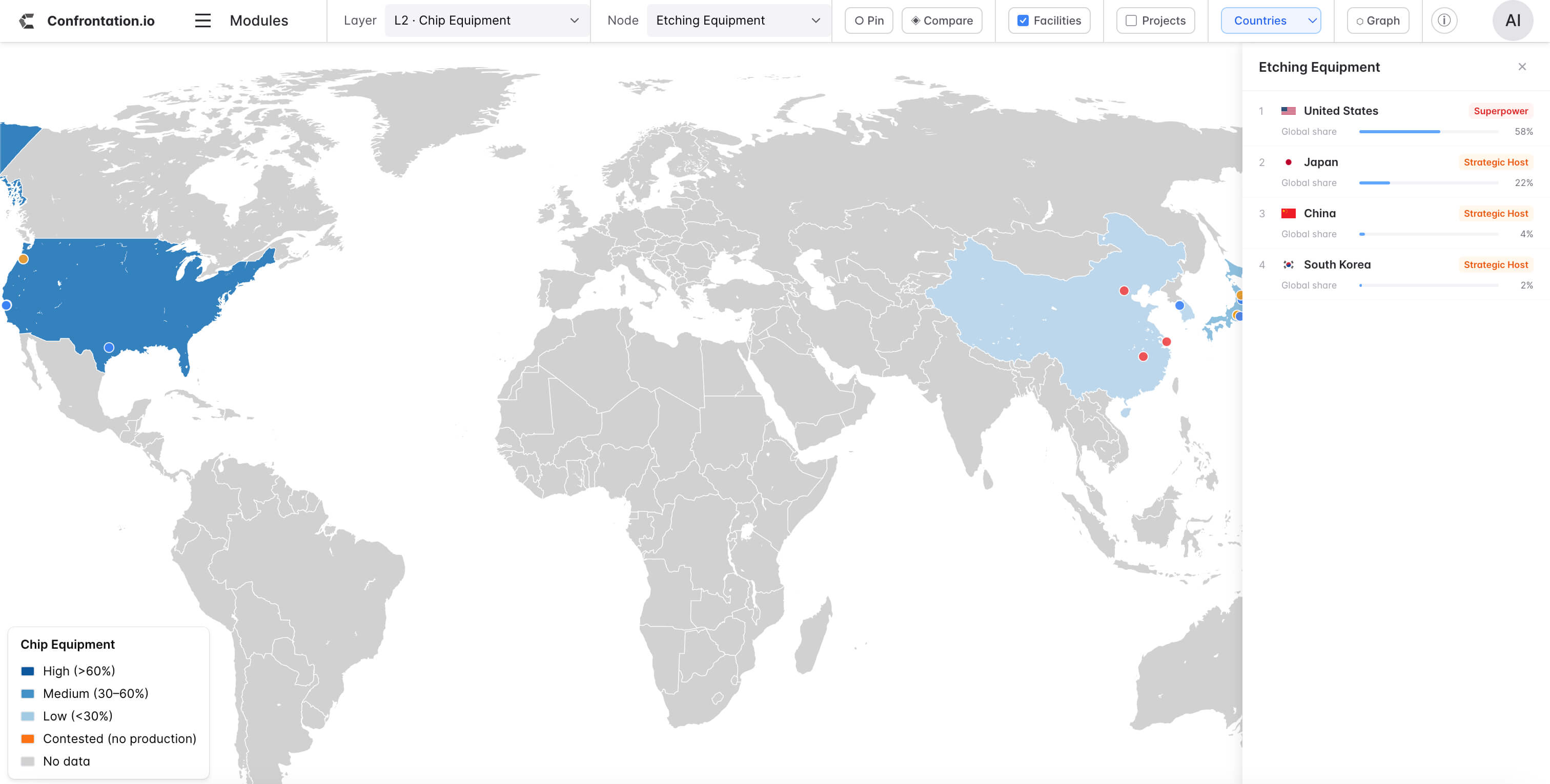
Applied Materials, based in the United States, is one of the most important companies in this area. Its equipment is used across materials engineering, deposition, surface modification, and several other stages of semiconductor manufacturing.
Lam Research, also based in the United States, has a particularly important position in etching.
Lithography determines where a pattern should appear. Etching helps transfer that pattern into the physical structure of the wafer by removing selected material with high precision.
As transistor structures become smaller and more complex, etching becomes more difficult. The process must remove material in exact locations without damaging adjacent structures or creating defects that reduce yield.
Tokyo Electron demonstrates Japan’s importance within the equipment chain.
The company supplies systems used in coating, developing, deposition, etching, cleaning, and other manufacturing processes. Japan is therefore not only a supplier of semiconductor chemicals and materials. It is also one of the leading producers of the machinery used inside fabrication plants.
Each equipment category requires specialized engineering.
A company that excels in lithography cannot automatically produce leading deposition tools. A deposition specialist cannot immediately reproduce inspection systems. The technical knowledge, patents, supplier networks, and customer relationships are different.
This specialization creates a manufacturing environment in which no single company supplies the complete factory.
Inspection, Metrology, and Process Control
Advanced semiconductor manufacturing depends on constant measurement.
A fabrication plant cannot wait until a processor is complete to determine whether production worked correctly. Defects must be identified throughout the process.
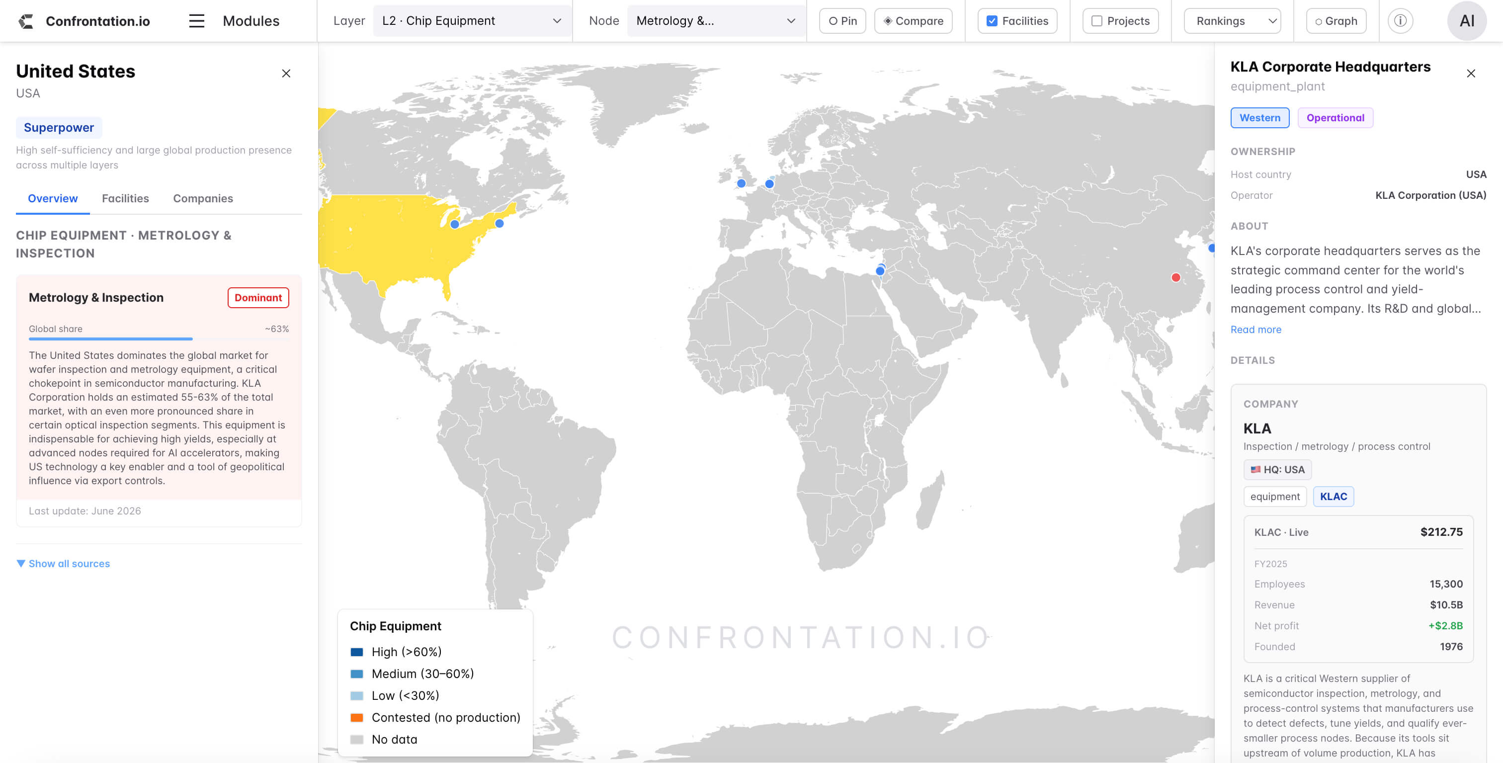
KLA occupies a central role in inspection, metrology, and process control.
Its systems examine wafers, measure patterns, identify contamination, detect structural defects, and help factories determine whether manufacturing equipment is operating within the required tolerances.
This layer receives less public attention than lithography, although it is essential to production economics.
A semiconductor factory is judged not only by whether it can produce an advanced chip, but by how many usable chips it can produce from each wafer. This is the manufacturing yield.
A process that creates functional processors only occasionally is not commercially competitive. High-volume production requires consistent output across large numbers of wafers.
Inspection data allows engineers to identify where defects are occurring and how the process must be adjusted. The factory continuously learns from its own production.
This creates an accumulated advantage.
A foundry that has operated an advanced manufacturing process for years develops a large body of process data, engineering routines, equipment settings, supplier knowledge, and defect-management experience.
This experience cannot be purchased as a single machine or transferred through a construction contract.
It becomes embedded in the operation of the factory.
Taiwan and the Manufacturing Machine
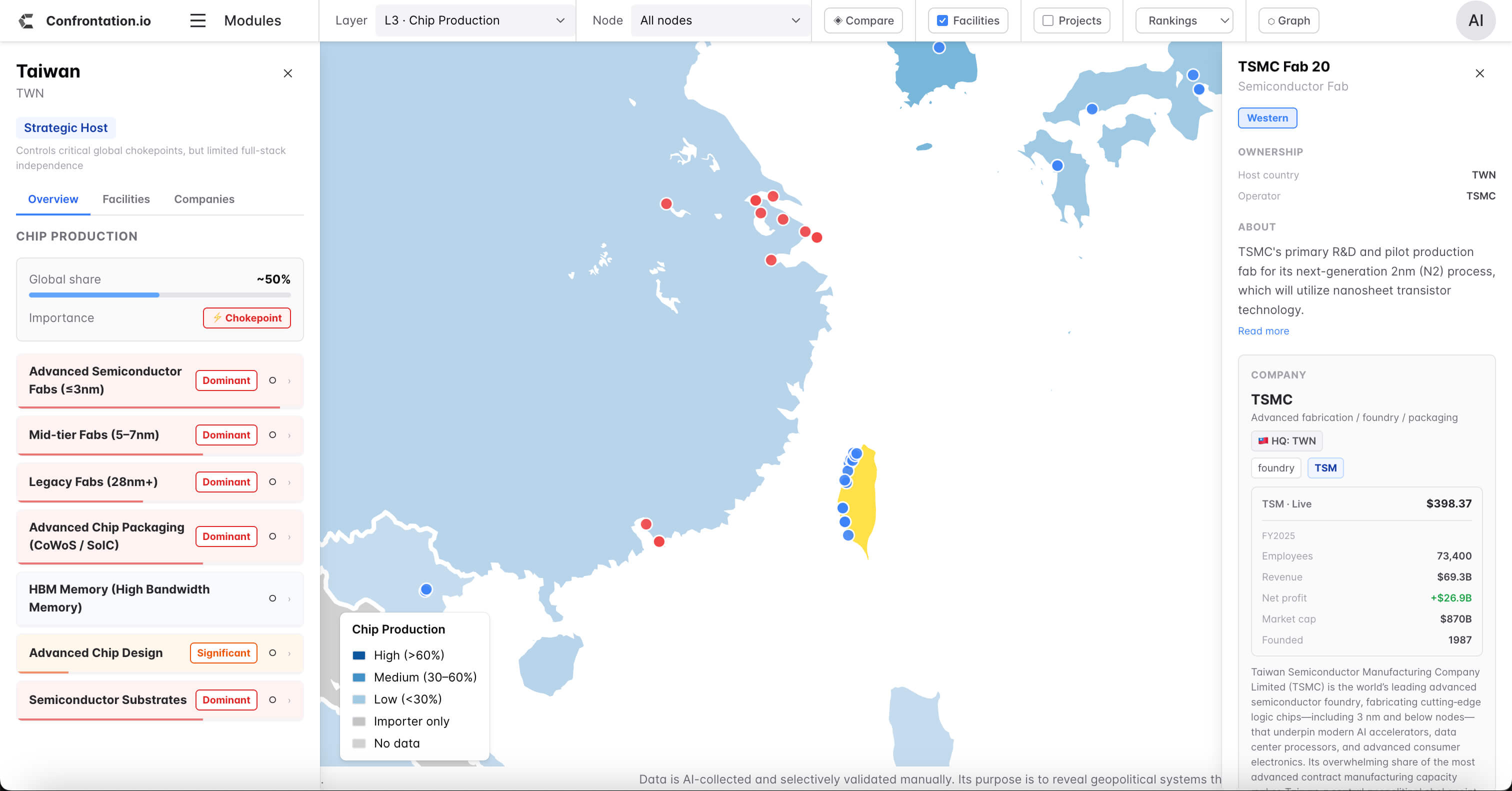
Taiwan is where the distributed semiconductor system becomes a physical product.
A chip designer can create an advanced blueprint. Equipment companies can supply the machines required to manufacture it. Chemical and material suppliers can provide the necessary inputs.
None of these elements independently creates an AI processor.
The central challenge is integrating all of them inside a fabrication plant capable of producing advanced chips with sufficient precision, volume, and yield.
TSMC fills this role.
Across Taiwan, the company operates a network of highly advanced semiconductor sites. These facilities are not conventional factories. They are tightly controlled production systems combining cleanrooms, lithography machines, chemical pipelines, automated wafer transport, deposition tools, etching systems, inspection equipment, utilities, software, and thousands of engineers.
The importance of TSMC does not come only from owning fabrication buildings.
It comes from coordinating the full manufacturing process.
Every stage must operate within precise limits. Materials must remain pure. equipment must be calibrated. contamination must be controlled. process steps must be repeated consistently. defects must be detected early. designs must be adapted to the production line.
This creates a deep form of industrial knowledge.
Taiwan’s position is therefore based on more than factory capacity. It hosts the most advanced manufacturing cluster in the semiconductor industry.
TSMC depends heavily on foreign inputs. Its facilities use design software from the United States and Europe, lithography systems from the Netherlands, optics and lasers from Germany, equipment from the United States and Japan, and materials from a wider supplier network.
The dependency also operates in the opposite direction.
Chip designers, cloud companies, equipment suppliers, and governments depend on Taiwan because TSMC integrates these international inputs into working processors.
This mutual dependency explains Taiwan’s position within the AI economy.
Taiwan does not independently control the full semiconductor chain. It controls the point at which much of the chain is brought together.
Diversifying Fabrication
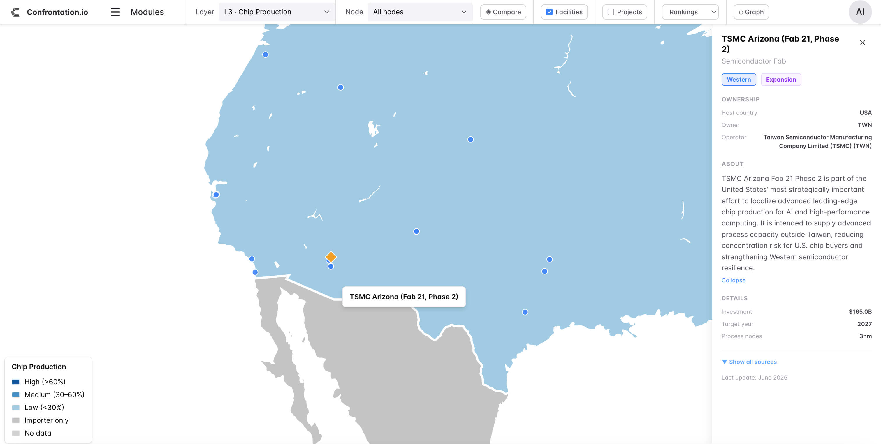
The concentration of advanced fabrication in Taiwan has led the United States, Japan, Europe, and other governments to support new semiconductor plants within their own territories.
The objective is to reduce exposure to geographic disruption, political conflict, natural disasters, logistics failures, and supply-chain interruptions.
The United States has supported major new investments in Arizona. Japan has encouraged new fabrication capacity in Kumamoto. European governments are financing semiconductor projects intended to strengthen domestic and regional production.
These investments can increase resilience. They can provide additional production capacity, create local supplier networks, and reduce dependence on a single geographic area.
They do not immediately replace Taiwan.
A fabrication plant is not simply a building containing expensive machines.
Advanced production depends on experienced engineers, specialized maintenance, reliable electricity and water, chemical suppliers, equipment technicians, logistics systems, customer relationships, process data, and an industrial culture capable of sustaining continuous improvement.
These capabilities develop over time.
A government can finance construction and subsidize equipment purchases. It cannot instantly reproduce decades of operational experience.
Diversification should therefore be understood as a gradual expansion of the manufacturing system rather than a direct relocation of Taiwan’s role.
The international semiconductor alliance is attempting to create more geographic redundancy while continuing to depend on Taiwan as its primary manufacturing anchor.
Advanced Packaging
The fabrication of the wafer does not complete the AI accelerator.
Once manufacturing is finished, the wafer is divided into individual processor dies. These dies must then be integrated with memory and other components.
Advanced packaging has become one of the most important layers of AI infrastructure.
Traditional packaging was often treated as a lower-value stage that occurred after the technologically difficult part of semiconductor production had been completed.
Modern AI systems have changed this structure.
An AI accelerator must move enormous volumes of data between the processor and memory. Performance depends not only on the speed of computation but also on the speed at which data can reach the processor.
If the accelerator is waiting for data, part of its computing capacity remains unused.
Advanced packaging reduces the physical distance between logic and memory, increases communication bandwidth, and allows several semiconductor components to operate as an integrated system.
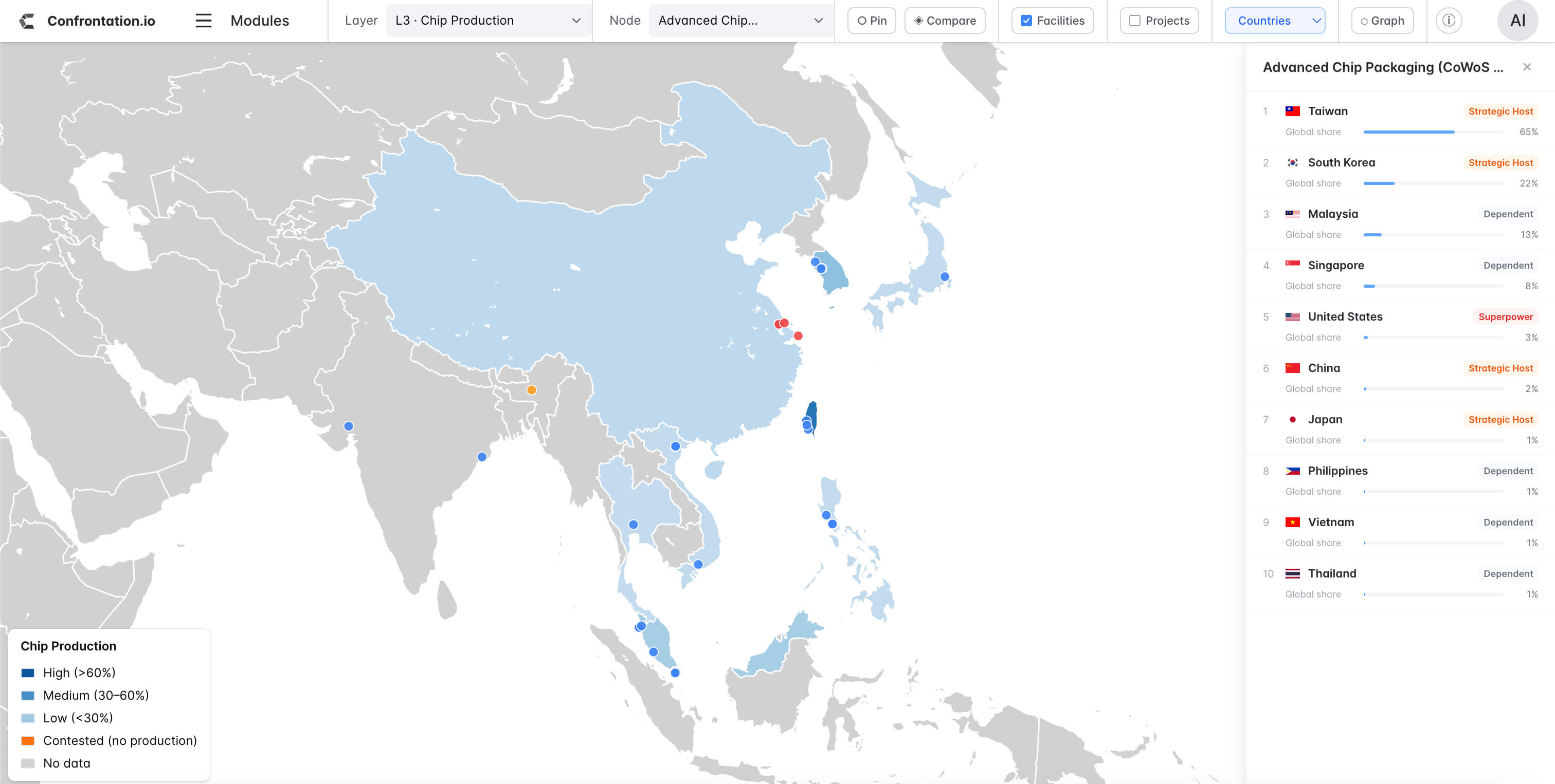
Taiwan is central to this layer through TSMC’s advanced packaging technologies, including CoWoS and SoIC.
These systems connect logic dies, memory stacks, substrates, and interposers into a high-performance package capable of supporting demanding AI workloads.
Packaging capacity has become a bottleneck because demand for AI accelerators increased faster than the available capacity to assemble them.
A fabrication plant may be able to produce the processor die, while the finished accelerator remains delayed because packaging capacity is unavailable.
This changes the strategic status of the industry.
Packaging is no longer treated only as a final assembly process. It influences how quickly AI computing capacity can be deployed.
High-Bandwidth Memory
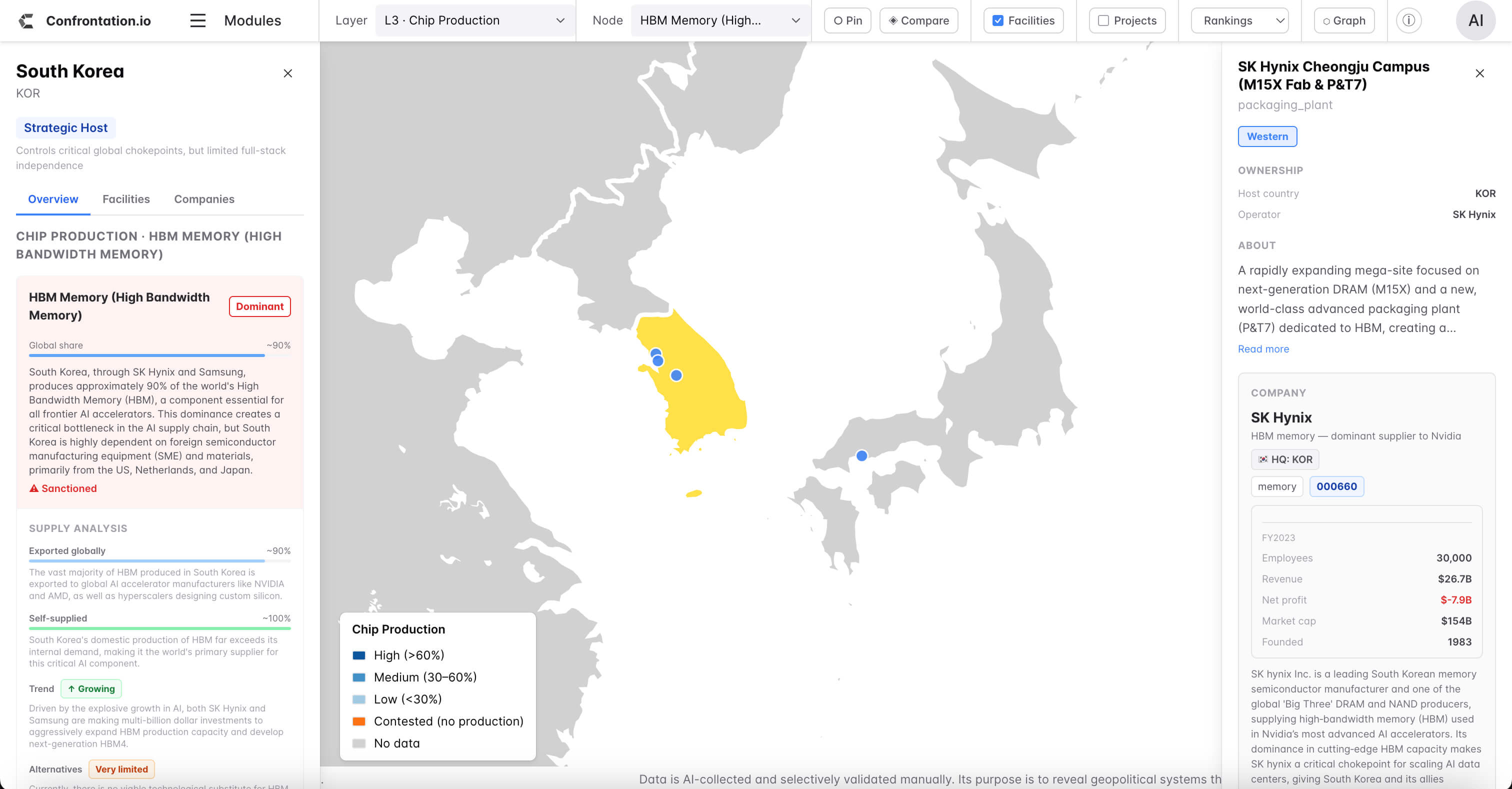
High-bandwidth memory creates another geographic dependency.
HBM is designed to deliver data to processors at much higher bandwidth than conventional memory configurations. Memory dies are stacked vertically and connected through advanced packaging techniques.
South Korean companies occupy leading positions in this market.
SK Hynix has become a particularly important supplier of HBM used in AI accelerators. Samsung is another major producer, while Micron provides an American source of advanced memory.
The finished AI accelerator therefore represents a combination of several national industrial systems.
The logic processor may be designed in the United States. The architecture may incorporate intellectual property developed in the United Kingdom. The design may be verified through American and German software. The wafer may be manufactured in Taiwan using Dutch lithography, German optics, American and Japanese equipment, and Japanese materials.
The HBM may come from South Korea or the United States. The processor and memory may then be assembled through advanced packaging in Taiwan.
No single company or country controls every stage.
The system works because specialized firms coordinate across borders.
This also means that replacing one supplier frequently requires changes elsewhere in the chain. A different memory provider may require package redesign. A different fabrication process may require changes to the chip layout. A different equipment configuration may affect materials, inspection, and manufacturing yields.
The chain is interconnected rather than modular.
From the Accelerator to the Data Center
The completed accelerator still does not produce AI capability on its own.
It must be installed in a server, connected to networking equipment, integrated into a data-center rack, powered continuously, and cooled.
Large AI training systems use clusters of accelerators operating together. Their performance depends on the ability to move data quickly across the cluster.
This creates demand for networking chips, optical links, switches, cables, storage systems, and communications equipment.
It also creates enormous electricity requirements.
The United States currently holds a major advantage in large-scale AI compute infrastructure because of its cloud companies, financial markets, technology ecosystem, available land, energy resources, and concentration of leading AI developers.
Other regions are investing rapidly.
Middle Eastern governments are financing data centers and computing capacity as part of broader strategies to diversify their economies and build influence within the AI sector.
European countries are supporting sovereign-compute projects, although electricity prices, permitting, grid constraints, and fragmented capital markets can slow development.
China continues to expand domestic computing infrastructure while facing restrictions on access to the most advanced foreign accelerators.
Several Asian economies are also building data-center capacity around existing semiconductor, electronics, and telecommunications industries.
The AI infrastructure chain therefore extends beyond chip manufacturing.
Electricity generation, transmission grids, cooling systems, water access, fiber networks, cloud platforms, and construction capacity all influence how quickly semiconductor output becomes usable AI compute.
An Industrial Alliance
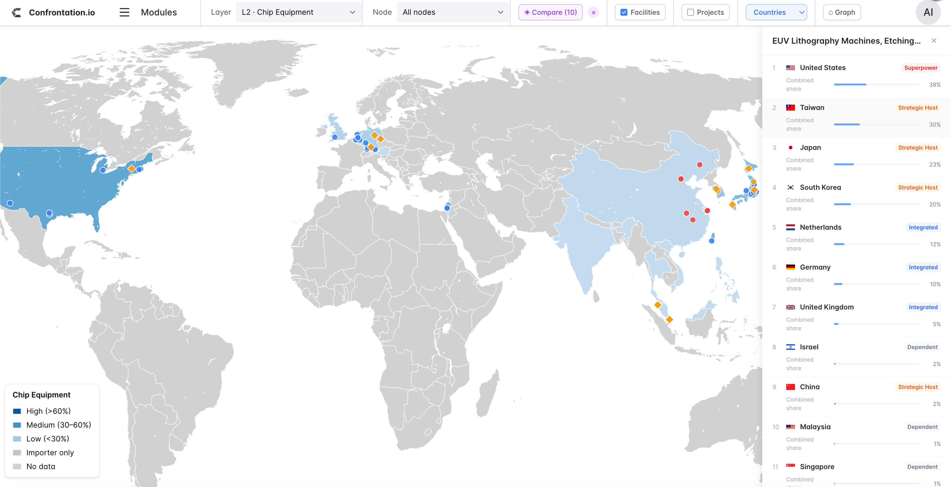
The semiconductor system resembles an alliance because each major region contributes a critical part of the production chain.
The United States contributes advanced processor design, EDA software, manufacturing equipment, cloud infrastructure, and much of the commercial demand for AI accelerators.
The United Kingdom contributes influential processor architecture and intellectual property.
The Netherlands supplies the central lithography platforms required for advanced manufacturing.
Germany contributes precision optics, laser systems, industrial equipment, and design software.
Japan supplies fabrication equipment, chemicals, photoresists, wafers, substrates, and specialized materials.
Taiwan provides the manufacturing and packaging system that integrates the wider chain.
South Korea supplies much of the advanced memory required to operate AI processors efficiently.
The alliance is not governed through a single institution. Its members do not share identical interests. Companies compete with one another, while governments pursue national industrial policies.
The system nevertheless functions as a coordinated network because each participant depends on the others.
A chip designed in the United States may require European software, Dutch lithography, German optics, Japanese equipment, Taiwanese fabrication, South Korean memory, and Taiwanese packaging.
The final product is global even when the company name printed on it is American.
Concentration and Fragility
The system’s efficiency comes from concentration.
Companies specialize in narrow technical areas and invest enormous amounts of capital in maintaining leadership. Customers rely on the most advanced supplier rather than supporting many less efficient alternatives.
This structure creates industrial chokepoints.
ASML occupies a unique position in advanced lithography. Zeiss has a central role in the optical systems used inside EUV machines. Synopsys, Cadence, and Siemens EDA dominate advanced chip-design software. Applied Materials, Lam Research, Tokyo Electron, and KLA hold important positions across fabrication equipment.
TSMC dominates leading-edge foundry production and advanced packaging. SK Hynix and Samsung are central to HBM production.
A disruption at any one of these points can affect the rest of the chain.
The risk may come from political conflict, export controls, natural disasters, industrial accidents, electricity shortages, logistics problems, cyberattacks, or sudden changes in demand.
The semiconductor alliance is therefore powerful but fragile.
It has extraordinary technical depth, although much of that depth is concentrated in a small number of companies and locations.
China’s Industrial Project
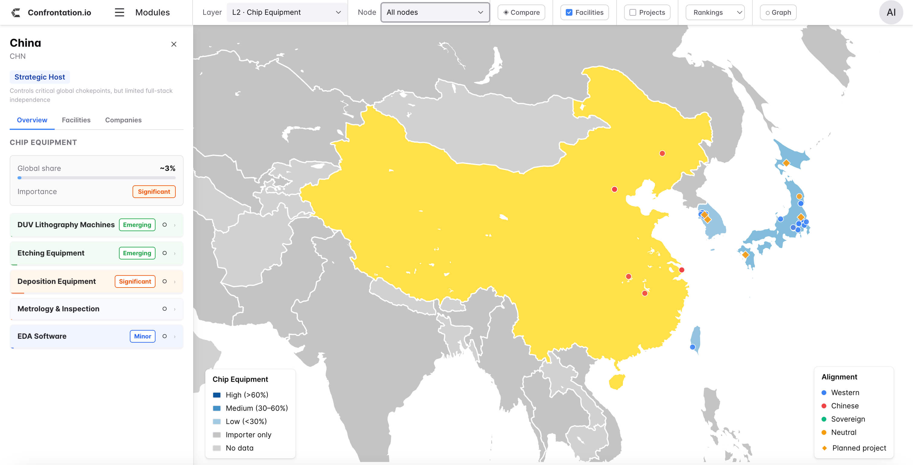
China’s semiconductor strategy is aimed at reducing dependence on this external system.
The objective is not simply to manufacture more chips.
China is attempting to build domestic alternatives across architecture, processor design, EDA software, lithography, deposition, etching, cleaning, inspection, fabrication, memory, packaging, and semiconductor materials.
Progress varies by layer.
China has developed substantial capabilities in chip design, mature-node manufacturing, packaging, communications semiconductors, power electronics, and several categories of fabrication equipment.
The largest remaining gaps are concentrated in the most advanced tools, software, processes, and components.
Lithography is the most visible challenge, although it is not the only one. Even a domestic lithography machine must operate alongside compatible optics, photoresists, masks, metrology systems, defect inspection, process software, and factory controls.
The problem is therefore systemic.
Reproducing a single machine does not reproduce the semiconductor ecosystem.
China must establish a network in which each domestic layer can operate reliably with the others. Equipment must reach commercial levels of performance. Foundries must learn how to integrate it. Chip designs must be adapted to domestic manufacturing processes. Suppliers must provide materials at consistent quality. Factories must achieve competitive yields.
None of these objectives is impossible in principle.
The difficulty lies in building many advanced industrial capabilities simultaneously while existing leaders continue to improve their own technologies.
China is not attempting to copy a static system. It is attempting to catch a system that continues to move.
Protecting and Expanding the Existing System
The United States and its allies are pursuing two strategies at the same time.
The first is protection.
Export controls, investment screening, licensing requirements, and technology restrictions are intended to limit the transfer of advanced chips, manufacturing equipment, software, and technical knowledge to strategic competitors.
These policies attempt to preserve the existing technological advantage of the allied semiconductor network.
The second strategy is diversification.
Governments are financing new fabs, packaging facilities, memory production, materials projects, research programs, and supplier capacity across the United States, Japan, Europe, and other partner economies.
The objective is to reduce the fragility created by geographic and corporate concentration.
These two strategies can conflict.
Protection encourages tighter control over technology. Diversification requires wider investment, more suppliers, and deeper cross-border coordination.
New factories can increase resilience, although they may also raise costs. Duplicating capacity across several countries is less economically efficient than concentrating production in the most competitive location.
Governments are increasingly willing to accept this cost because semiconductor capacity is no longer viewed as a purely commercial asset.
It is treated as national infrastructure.
Two Competing Industrial Models
The semiconductor conflict is often simplified into a competition between the West and China.
The deeper structure consists of two different industrial projects.
The United States and its allies are attempting to protect and expand a distributed semiconductor system. Their advantage comes from specialization across many countries and companies.
China is attempting to internalize more of the chain. Its objective is to reduce exposure to foreign bottlenecks by developing domestic alternatives across a wider range of technologies.
The distributed model benefits from access to the strongest specialist in each category. It can combine Dutch lithography, German optics, American software, Japanese equipment, Taiwanese manufacturing, and Korean memory.
Its weakness is dependency on cross-border coordination and political stability.
The domestic model offers greater strategic autonomy if it succeeds. Its weakness is the enormous difficulty of reproducing many specialized industries within one national system.
The likely outcome is not complete separation.
A more probable result is partial duplication, higher inventories, greater government financing, stronger preference for politically aligned suppliers, and a gradual division of the semiconductor industry into competing technological blocs.
Implications for the AI Race
Semiconductors are central to AI because every model ultimately depends on physical computing infrastructure.
Before an AI system becomes software, it must pass through architecture, design, simulation, lithography, fabrication, inspection, memory integration, packaging, server manufacturing, networking, electricity, and cooling.
Restrictions or shortages at any of these layers can influence the cost and speed of AI development.
A shortage of advanced accelerators can delay data-center construction. Limited HBM supply can constrain processor output. Packaging bottlenecks can slow delivery even when logic dies are available. Electricity constraints can prevent completed servers from being deployed.
The AI race is therefore not determined only by algorithmic research.
It depends on the ability to coordinate a large industrial system.
Countries that control several parts of this system gain influence over the pace at which AI capabilities can expand. Countries that depend on external suppliers remain exposed to export controls, supply interruptions, and political pressure.
This is why semiconductor policy has moved beyond ordinary industrial policy.
It now affects economic competitiveness, military capacity, cloud infrastructure, scientific research, intelligence systems, and national security.
Conclusion
An AI chip is not the product of one company or one country.
It is the physical output of a distributed industrial alliance.
The architecture and design layers are concentrated in the United States and the United Kingdom. The software layer depends on a small group of American and European companies. Advanced lithography combines Dutch systems, German optics and lasers, and American technology.
The wider fabrication-equipment chain depends on companies in the United States and Japan. Taiwan integrates these tools through advanced manufacturing and packaging. South Korea supplies much of the high-bandwidth memory required by modern AI systems.
The finished accelerator carries the accumulated knowledge of this entire network.
This structure gives the alliance extraordinary technological power. It also creates narrow points of concentration that can become economic and geopolitical vulnerabilities.
China’s semiconductor program is an attempt to reduce dependence on a system it does not fully control. The United States and its allies are attempting to preserve their technological advantages while making the existing network more geographically resilient.
The resulting competition will not be decided by one chip, one factory, or one lithography machine.
It will depend on which industrial system can build, coordinate, protect, and scale the full chain more effectively.
The AI race begins with chips.
The chips begin with the alliance behind them.